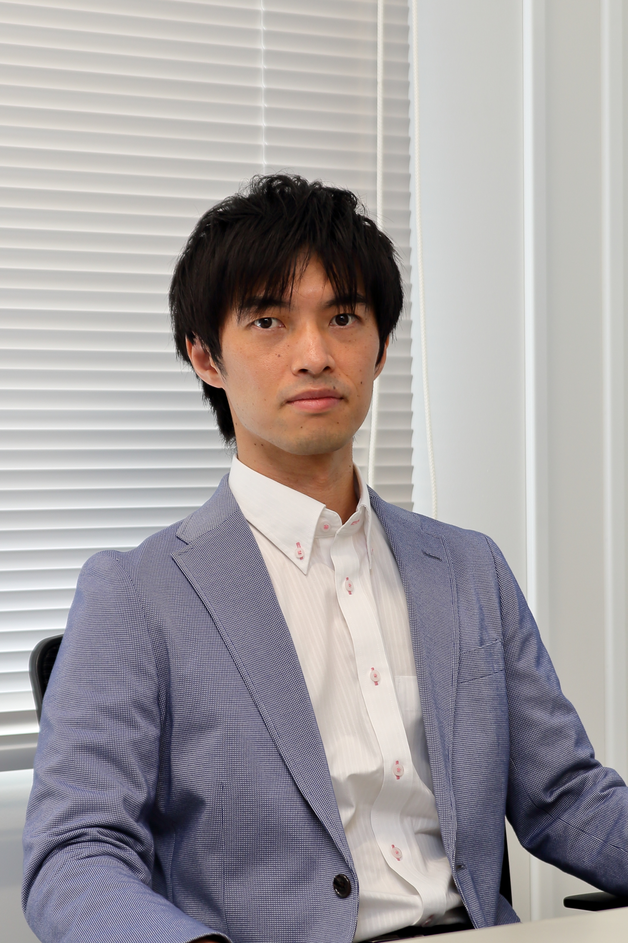
|
Affiliation |
Institute for Multidisciplinary Sciences |
|
Job Title |
Professor |
|
Research Fields, Keywords |
Unit processes for 3D integration, advanced packaging |
|
Web Site |
|
|
Related SDGs |
INOUE Fumihiro
|
|
|
Degree 【 display / non-display 】
-
Doctor of Engineering - Kansai University
Campus Career 【 display / non-display 】
-
2026.4
Duty Yokohama National UniversityInstitute for Multidisciplinary Sciences Professor
-
2021.4-2026.3
Duty Yokohama National UniversityFaculty of Engineering Division of Systems Research Associate Professor
-
2026.4
Concurrently Yokohama National UniversityInstitute for Multidisciplinary Sciences Professor
-
2026.4
Concurrently Yokohama National UniversityInstitute of Advanced Sciences Professor
-
2024.4-2026.3
Concurrently Yokohama National UniversityInstitute for Multidisciplinary Sciences Associate Professor
External Career 【 display / non-display 】
-
2011.3-2014.10
imec
-
2013.4-2014.10
Tohoku University Special researcher of the Japan Society for the Promotion of Science
-
2014.10-2021.3
imec Researcher
Books 【 display / non-display 】
-
Exploring Bond Strength for Advanced Chiplet with Hybrid Bonding
Fuse, J.; Iwata, T.; Yoshihara, Y.; Sano, M.; Inoue, F.( Role: Joint author , vol28, (1) 39-45)
Chip Scale Review
Language:English Book type:Scholarly book
Papers 【 display / non-display 】
-
Assessment of the Indium Chemical Mechanical Polishing Mechanism via Corrosion Analysis
La, MTN; Otake, Y; Inoue, F
JOURNAL OF THE ELECTROCHEMICAL SOCIETY 173 ( 3 ) 2026.2
Language:English Publishing type:Research paper (scientific journal) Joint Work
-
Measurement Methods of Within-Wafer Bond Strength Uniformity for Hybrid Bonding
KOBAYASHI Daiki, FUSE Junya, SANO Marie, YOSHIHARA Yuki, INOUE Fumihiro, KONDO Yusuke
Journal of Smart Processing 15 ( 1 ) 31 - 35 2026.1
Language:Japanese Publishing type:Research paper (scientific journal) Publisher:Smart Processing Society for Materials, Environment & Energy (High Temperature Society of Japan) Joint Work
-
Uedono, A; Hasunuma, R; Kitagawa, H; Yoshihara, Y; Inoue, F; Mihara, K; Aoki, S; Hare, T; Mori, K; … Show more authors
Uedono, A; Hasunuma, R; Kitagawa, H; Yoshihara, Y; Inoue, F; Mihara, K; Aoki, S; Hare, T; Mori, K; Murugesan, M; Fukushima, T Hide authors
ACS APPLIED ELECTRONIC MATERIALS 7 ( 23 ) 10761 - 10767 2025.12
Language:English Publishing type:Research paper (scientific journal) Joint Work
-
La, MTN; Otake, Y; Goundar, JA; Inoue, F
JOURNAL OF THE ELECTROCHEMICAL SOCIETY 172 ( 12 ) 2025.12
Language:English Publishing type:Research paper (scientific journal) Joint Work
-
Disaggregation and Re-Integration: Emerging Trends in Semiconductor Integration with Chiplets
Inoue Fumihiro
Journal of The Japan Institute of Electronics Packaging 28 ( 6 ) 511 - 515 2025.9
Language:Japanese Publishing type:Research paper (scientific journal) Publisher:The Japan Institute of Electronics Packaging Single Work
Review Papers 【 display / non-display 】
-
Assessing Queue Time in D2W Hybrid Bonding Through Precise Bond Strength Measurements
Yuki, Y; Fuse, J; Aoki, S; Hare, T; Mihara, K; Miyoshi, T; Yamamoto, N; Teranishi, S; Fukushima, T; … Show more authors
Yuki, Y; Fuse, J; Aoki, S; Hare, T; Mihara, K; Miyoshi, T; Yamamoto, N; Teranishi, S; Fukushima, T; Uedono, A; Inoue, F Hide authors
2025 IEEE 75TH ELECTRONIC COMPONENTS AND TECHNOLOGY CONFERENCE, ECTC 878 - 884 2025
Language:The in addition, foreign language Publishing type:Article, review, commentary, editorial, etc. (bulletin of university, research institution) Joint Work
-
Wet-chemical Cu Cleaning for Fine-Pitch Hybrid Bonding
Nakayama, K; Hayama, K; Tanaka, F; Dewilde, S; Deckers, S; Heylen, N; Tanaka, Y; Okazaki, Y; Gan, N … Show more authors
Nakayama, K; Hayama, K; Tanaka, F; Dewilde, S; Deckers, S; Heylen, N; Tanaka, Y; Okazaki, Y; Gan, N; Iino, H; Inoue, F; Philipsen, H Hide authors
2025 IEEE 75TH ELECTRONIC COMPONENTS AND TECHNOLOGY CONFERENCE, ECTC 1859 - 1863 2025
Language:The in addition, foreign language Publishing type:Article, review, commentary, editorial, etc. (bulletin of university, research institution) Joint Work
-
Novel Bonding Interfacial Material for Carrier Wafer of BSPDN & Reconstructed D2W Integration
Kitagawa, H; Yamamoto, T; Lee, J; Machida, S; Yuasa, K; Inoue, F
2025 IEEE INTERNATIONAL INTERCONNECT TECHNOLOGY CONFERENCE, IITC 2025
Language:The in addition, foreign language Publishing type:Article, review, commentary, editorial, etc. (bulletin of university, research institution) Joint Work
-
Material-Mechanistic Interplay in SiCN Wafer Bonding for 3D Integration
Kitagawa, H; Sato, R; Ebiko, S; Nagata, A; Ahn, C; Kim, Y; Kang, J; Uedono, A; Inoue, F
ACS OMEGA 10 ( 25 ) 27575 - 27584 2025
Language:The in addition, foreign language Publishing type:Article, review, commentary, editorial, etc. (bulletin of university, research institution) Joint Work
-
Factors determining bond wave speed in wafer bonding
Sato, R; Nagata, A; Kitagawa, H; Ogata, R; Myalitsin, A; Inoue, F
JAPANESE JOURNAL OF APPLIED PHYSICS 64 ( 3 ) 2025
Language:The in addition, foreign language Publishing type:Article, review, commentary, editorial, etc. (bulletin of university, research institution) Joint Work
Awards 【 display / non-display 】
-
2024.7 産経新聞社 ハイブリッド接合の開発と省電力チップレット集積技術への適用
Individual or group name of awards:井上史大
-
令和6年度科学技術分野の文部科学大臣表彰【若手科学者賞】
2024.4 文部科学省
Individual or group name of awards:井上史大
-
IEEE EPS Outstanding Young Engineer Award
2022.6 IEEE Electronics Packaging Society
Individual or group name of awards:Fumihiro Inoue
-
SEMIスタンダード:2025年テクニカルコミッティー賞
2026.1 SEMI Japan
Individual or group name of awards:井上史大
-
JAFOE2025 Best Speaker Award
2026.1 Engineering Academy of Japan
Individual or group name of awards:Fumihiro Inoue
Preferred joint research theme 【 display / non-display 】
-
3D integration
-
Semiconductor manufacturing processes
-
Hybrid bonding
-
CMP
-
Electrochemical deposition
Charge of on-campus class subject 【 display / non-display 】
-
2026 Advanced Semiconductor Manufacturing
Interfaculty Graduate School of Innovative and Practical Studies
-
2026 Micro and nanofabrication
Graduate school of Engineering Science
-
2026 Studio of Process Integration B
Graduate school of Engineering Science
-
2026 Studio of Process Integration A
Graduate school of Engineering Science
-
2026 Manufacturing of Processing Systems B
Graduate school of Engineering Science
Media Coverage 【 display / non-display 】
-
チップレット集積の課題は山積み、うかうかできない日本企業
日経BP 日経XTECH 2024.2
Author:Other
-
「後工程から日本の半導体を盛り返したい」…横浜国立大准教授が3D集積技術に挑む
日刊工業新聞 日刊工業新聞 ニュースイッチ 2024.2
Author:Other


 ORCID
ORCID
